Advanced semiconductor packaging technologies like 2.5D and 3D hybrid bonding, along with emerging solutions like silicon photonics, are critical in optimizing system performance and fostering the next wave of AI and HPC chip innovation. The “Advanced Semiconductor Packaging 2024-2034: Forecasts, Technologies, Applications” report recently published by IDTechEx explores the evolving landscape of semiconductor packaging, with a focus on 2.5D and 3D hybrid bonding packaging. It covers technology trends, industry challenges, and the advancements made by key players while forecasting market trends in the semiconductor packaging sector.
Large Language Models (LLM) challenges:
The emergence of large language models (LLMs) marks a milestone in AI, revolutionizing natural language processing (NLP) and related fields. Models like OpenAI’s GPT series demonstrate high accuracy in understanding, generating, and translating human language. While they find diverse applications, they also present challenges.
LLMs have seen exponential growth in the model size, from 340 million parameters in BERT-L in 2019 to 1.76 trillion parameters in the upcoming GPT-4. This expansion results in high computational complexity, with GPT-4 requiring over 1010 petaFLOPS. Compared to other neural networks, LLMs demand significantly more computational resources; for instance, training GPT-3 takes 3841 GPU hours versus 11 hours for a ResNet-60 (a convolutional neural network used for image classification). LLMs have low operational intensity, meaning they rely heavily on matrix-vector operations. This requires moving more data to perform the same number of arithmetic operations. Memory bandwidth is thus critical for their performance.
Ways to improve system bandwidth:
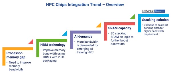
In recent years, there’s been a gap between the rapid rise in processor compute density and the slower increase in memory bandwidth. This “memory wall” issue results in processors frequently waiting for data, leading to underutilization and posing a substantial challenge to future performance improvements.
NVIDIA and AMD have introduced NVLink and Infinity Fabric technology, respectively, to enhance CPU-GPU interconnectivity, which is crucial for improving bandwidth between logic components.
The incorporation of next-generation High Bandwidth Memories (HBMs), which consist of multiple vertically stacked DRAM dies connected by through-silicon vias (TSVs), into architectures offers a substantial boost in logic-to-memory bandwidth. While previously confined to GPUs, HBMs are now being integrated with CPUs, bridging the bandwidth gap between CPU and traditional DRAM. AMD’s Instinct MI300 exemplifies this trend by integrating advanced HBMs with both CPU and GPU in a single package. 2.5D semiconductor packaging technologies like TSMC’s Chip on Wafer on Substrate (CoWoS) play a crucial role in increasing the number of I/O (Input/Output) points while reducing interconnect length between logic and memory components, enhancing performance and reducing latency. However, emerging HPC workloads, particularly those related to AI training, demand even higher memory bandwidth (over 45x) due to frequent memory accesses. Increasing I/O speed can indeed enhance HBM’s bandwidth, but it’s limited due to increased power consumption.
To address this, new processor designs have focused on increasing on-chip SRAM capacity, as it’s situated near the processing chips, enabling higher bandwidth with denser interconnects and lower latency. Initial implementations used 3D hybrid bonding packaging technology to bond an SRAM die over a logic die at a 9 μm pitch, tripling SRAM capacity. Further bandwidth improvements involve continuously decreasing the hybrid bonding pitch from 9 μm to 0.4 μm, leading to a substantial over 300-fold increase in bandwidth density.
Co-packaged optics is another approach that is gaining significant momentum in recent years. Optical communication offers several advantages over traditional electrical signal transmission. It boasts lower transmission loss, reducing signal degradation over distances. Furthermore, optical communication is less susceptible to crosstalk, which occurs when signals interfere with each other, leading to data errors. Additionally, optical signals can achieve higher bandwidth compared to their electrical counterparts, making them ideal for data-intensive applications.
To summarize, for the next generation AI compute system, high logic-to-logic and logic-to-memory bandwidth are crucial development trends. Advanced semiconductor packaging technologies like 2.5D and 3D hybrid bonding, alongside emerging solutions like optical communication, are pivotal for enabling this growth and overcoming computational challenges.
IDTechEx’s new report, “Advanced Semiconductor Packaging 2024-2034: Forecasts, Technologies, Applications“, delves into the dynamic landscape of 2.5D and 3D packaging, analyzing technology trends, industry barriers, key player’s technology roadmap, and market forecasts. Gain invaluable insights into not just AI and HPC applications but also 5G/6G, autonomous vehicles, and consumer electronics sectors, understanding how advanced packaging shapes their trajectory. With unbiased analysis and detailed market evaluations, this report provides a comprehensive understanding of the industry’s future, making it essential reading for stakeholders navigating the evolving semiconductor landscape.
To find out more about this IDTechEx report, including downloadable sample pages, please visit www.IDTechEx.com/ASP.
About IDTechEx
IDTechEx guides your strategic business decisions through its Research, Subscription and Consultancy products, helping you profit from emerging technologies. For more information, contact research@IDTechEx.com or visit www.IDTechEx.com.
Images download:
https://www.dropbox.com/scl/fo/kiiebdhm6cy882lh4qumv/h?rlkey=6dmye7mfuki413i63h9j5wy9y&dl=0
Media Contact:
Lucy Rogers
Sales and Marketing Administrator
press@IDTechEx.com
+44(0)1223 812300
Social Media Links:
Twitter: www.twitter.com/IDTechEx
LinkedIn: www.linkedin.com/company/IDTechEx
Photo – https://mma.prnewswire.com/media/2342581/IDTechEx.jpg
Logo – https://mma.prnewswire.com/media/478371/IDTechEx_Logo.jpg
SOURCE IDTechEx


